In 1959, Richard Feynman gave a visionary talk entitled "There's Plenty of Room at the Bottom". He asked the question whether it will be possible to shrink devices all the way down to the atomic level. Since he could not find any law of physics against that, he concluded that is must be possible and will be done some day. In his characteristic way he went on to muse about all the neat things that one could do on such a scale. He started out with an atomic memory. Allowing 5x5x5=125 atoms to store one bit he estimated that all printed information accumulated over centuries since the Gutenberg Bible could be stored in a cube of material 1/200" = 0.1 mm wide, which is the barely visible to the naked eye. The ultimate storage medium would store one bit in a single atom, with a few atomic spacings between bits in order to keep them apart.
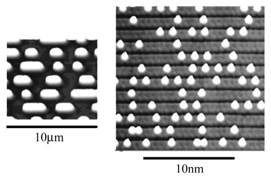
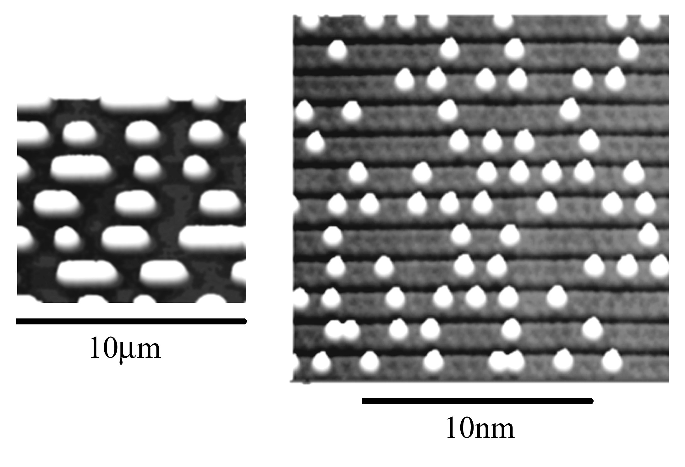
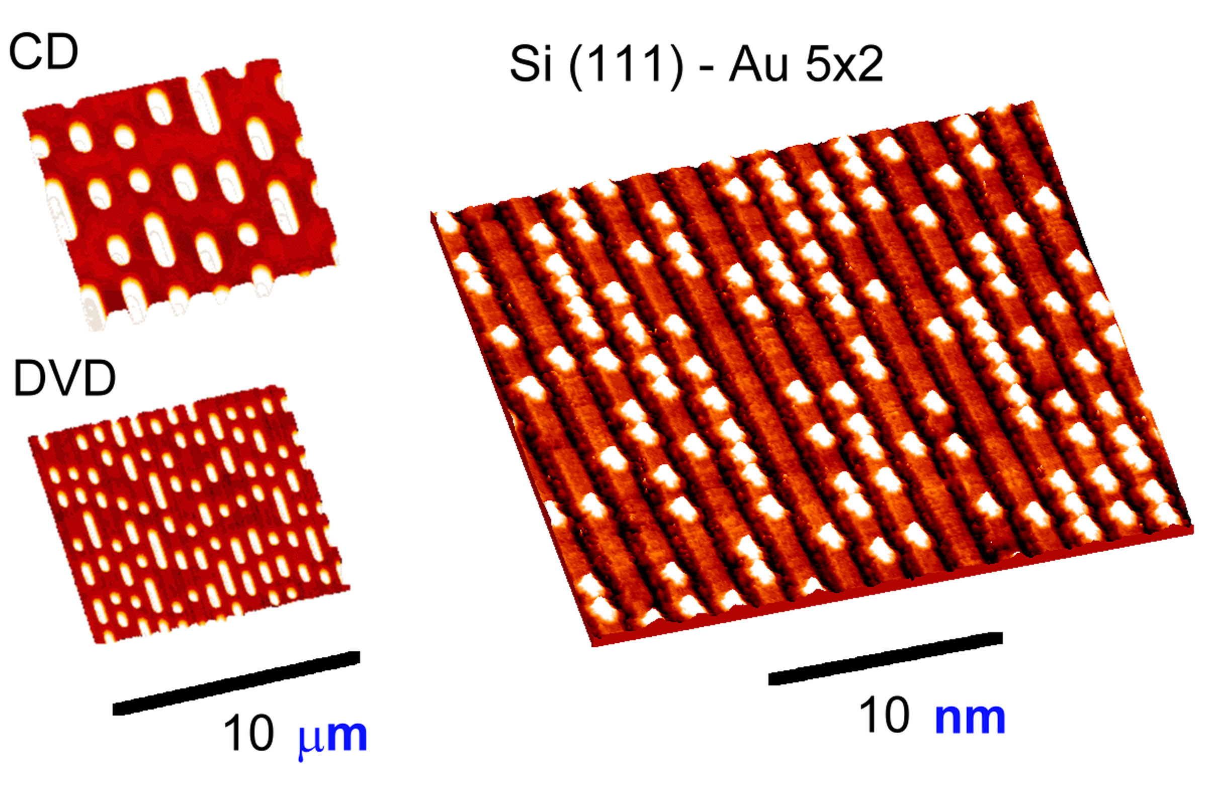
How far have we come forty years later? A two-dimensional version of Feynman's atomic
memory can be formed on the surface of silicon by a small amount of gold (below on the right).
It looks similar to the CD-ROM on the left, but the scale is in nanometers instead
of micrometers. Thefore, the storage density is a million times higher.
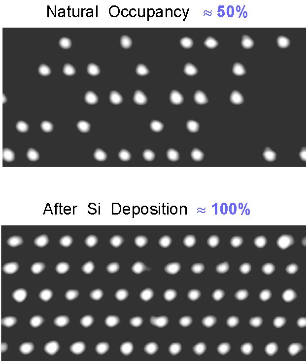
The gold triggers the formation of self-assembled tracks, which are exactly five atoms wide.
Extra silicon atoms sit on top of the tracks in well-defined positions. It is suggestive to assign an extra silicon atom to a
1 and a vacancy to a 0. The minimum empty area required around each bit is 5x4=20 atoms,
4 atoms along the track and 5 atoms from one track to the next. Feynman's 1959 suggestion of
spacing the bits 5 atoms apart was right on the mark.
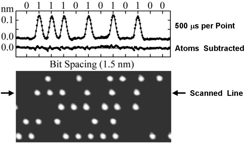
Reading the memory consists of a simple, line scan with a scanning tunneling microscope (STM) along the
self-assembled tracks. There is no need to search in two dimensions for the location of a bit.
The signal is highly predictable since all atoms have the same shape and sit on well-defined
lattice sites. That allows for a high level of filtering and error correction.
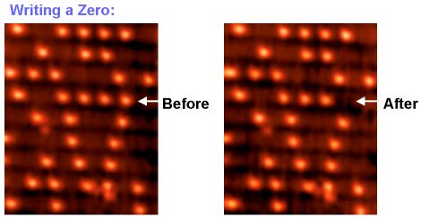
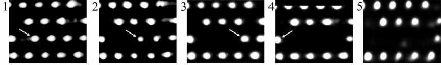
Writing is more difficult. While loosely-attached surface atoms can be moved around with a STM at liquid helium temperature, that is much harder to achieve that at room temperature. In order to prevent them from moving around spontaneously, it is necessary to choose atoms that are strongly bound to the surface. Pushing them around with the STM tip requires a close approach and often leads to atoms jumping over to the tip. This problem can be turned into a solution by using the STM tip to remove a silicon atom for writing a 0. The memory is pre-formatted with 1 everywhere by depositing silicon atoms onto all vacant sites.
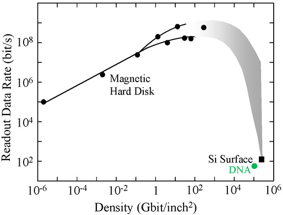
A storage device at the single atom limit can tell us something about how today's data storage might evolve in the future. The graph below shows readout speed versus storage density, two key properties of a memory. Compared to traditional data storage in hard disks, the silicon atom memory has a very impressive density (250 Terabits per square inch), but its data rate is extremely low. As the size of a bit shrinks, less energy that can be extracted from it during readout. Therefore, one needs a longer integration time for obtaining an acceptable signal-to-noise level. Even the theoretical limit of the data rate with the best possible readout electronics (top of the shaded region) is still lower than what hard disks achieve today. In the future, we may see a trade-off between density and speed. Actually, the data rate of hard disks shows signs of leveling out already. The data rate will have to be recovered by by a high degree of parallelism, for example large arrays of reading heads.
How does nature do it?
The figure below contains a green data point for DNA, nature's device for storing data.
DNA needs 32 atoms to store one bit, which is comparable to the area of 5x4=20 sites needed for a bit at a silicon surface.
The data rates are comparable, too.
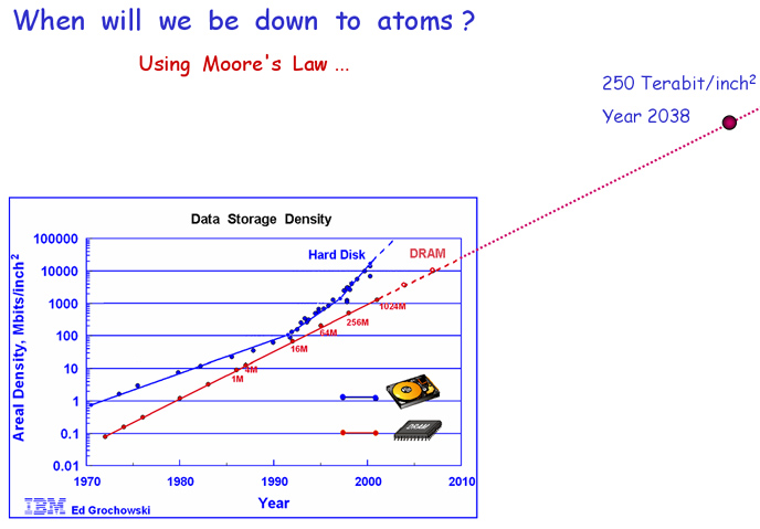
Will single atoms ever be used to store data?
Hard to tell. If Moore's law of silicon technology holds up,
one can use it to extrapolate the density of current silicon-based memory (DRAM in the figure below).
A memory with the density demonstrated here would then be commercialized in the year 2038. That is a daunting extrapolation.
What about storing one bit in a single spin?
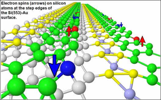
It has become possible to detect a single spin at a surface
with spin-polarized scanning tunneling microscopy. Recently, we have found that stepped silicon surfaces
decorated with gold are able to form lines of spins at the the step edges (see the end of the section on
ultimate nanowires). Such a single spin memory can be viewed as the ultimate hard disk,
in the same way as the single-atom silicon memory represents the ultimate DRAM. It is more difficult to
predict hard disk technology, though, because it does not evolve along a straight line in the figure above.
Images:
Large Images: