Semiconductor Surfaces/Interfaces
The Si/SiO2 Interface: A Classic
One of the main reasons for the dominant role of silicon technology is the extremely high electrical quality of the Si/SiO2 interface. Only 1
in 100,000 interface atoms is electrically active. Despite highly-developed device applications of silicon, the actual atomic bonding at the Si/SiO2 interface is not unique. The disordered (amorphous) structure of SiO2 allows many configurations and prevents the use of standard crystallographic techniques.
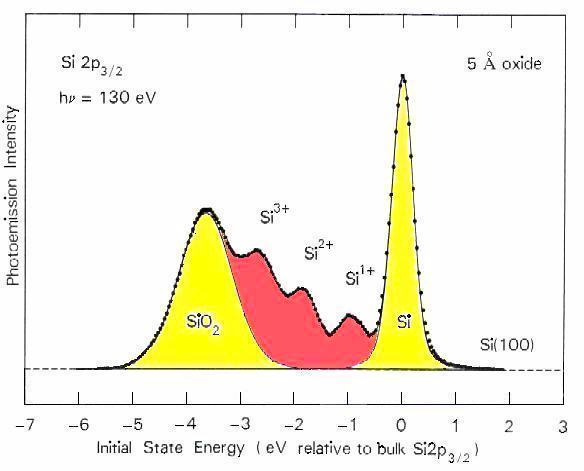
Core level spectroscopy makes it possible to reveal characteristic bonding configurations of silicon atoms at the interface. These are identified by detecting the energy shifts of the silicon 2p level induced by the bonding partners of a particular silicon atom. The figure shows that silicon atoms bonding to 0, 1, 2, 3, and 4 oxygens exhibit distinct energy shifts. Surprisingly, the intermediate oxidation states 1+, 2+, 3+ are found (in red). They are are unstable in bulk form, disproportionating into Si plus SiO2. At the interface, such a bond arrangement is forced upon the silicon atoms by the fact that they have to bond to silicon on one side of the interface and to oxygen on the other. The distribution of oxidation states changes with the preparation conditions and with the quality of the interface. This has led to widespread use in diagnostics of Si-oxide interfaces. Even after replacing SiO2 by other oxides with higher dielectric constant, the interface still involves silicon-oxygen bonds.
Synchrotron radiation
optimizes the sensitivity to detecting 1-2 monolayers of silicon atoms at the interface.
A widely-cited reference: F.J. Himpsel et al., Phys. Rev. B 38, 6084 (1988).

Diamonds Forever !
Wide-gap semiconductors, such as diamond and silicon carbide, are suitable for high power devices that still operate at high temperatures.
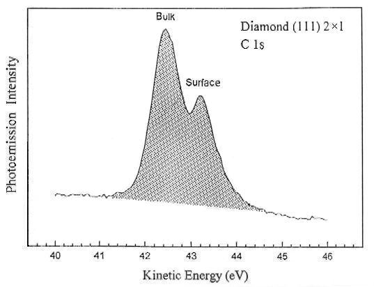
The figure below shows the energy shift of the carbon 1s level between sigma-bonded bulk diamond and pi-bonded carbon atoms at a clean surface. Synchrotron radiation is used again to optimize the signal from the outermost layer of carbon atoms.

Diamond also exhibits an unusual negative electron affinity, when the surface is terminated by hydrogen atoms. That makes it an efficient electron emitter. Excited electrons all trickle down to the bottom of the conduction band and escape from there. This is also true for thin diamond films, which are inexpensive to grow for devices.
A widely-cited reference: F.J. Himpsel et al., Phys. Rev. B 20, 624 (1979).
Franz Himpsel's Home Page